Lg 26lh20 Ua Chassis La92a l722h
This document was ed by and they confirmed that they have the permission to share it. If you are author or own the copyright of this book, please report to us by using this report form. Report l4457
Overview 6h3y3j
& View Lg 26lh20 Ua Chassis La92a as PDF for free.
More details h6z72
- Words: 7,590
- Pages: 31
Internal Use Only North/Latin America Europe/Africa Asia/Oceania
http://aic.lgservice.com http://eic.lgservice.com http://biz.lgservice.com
LCD TV SERVICE MANUAL CHASSIS : LA92A
MODEL : 26LH20
26LH20-UA
CAUTION BEFORE SERVICING THE CHASSIS, READ THE SAFETY PRECAUTIONS IN THIS MANUAL.
CONTENTS
CONTENTS ............................................................................................. 2 PRODUCT SAFETY ................................................................................. 3 SPECIFICATION ....................................................................................... 6 ADJUSTMENT INSTRUCTION ................................................................ 9 TROUBLE SHOOTING .......................................................................... 14 BLOCK DIAGRAM.................................................................................. 20 EXPLODED VIEW .................................................................................. 21 SVC. SHEET ...............................................................................................
Copyright C 2009 LG Electronics. Inc. All right reserved. Only for training and service purposes
-2-
LGE Internal Use Only
SAFETY PRECAUTIONS IMPORTANT SAFETY NOTICE Many electrical and mechanical parts in this chassis have special safety-related characteristics. These parts are identified by in the Schematic Diagram and Exploded View. It is essential that these special safety parts should be replaced with the same components as recommended in this manual to prevent Shock, Fire, or other Hazards. Do not modify the original design without permission of manufacturer.
Leakage Current Hot Check (See below Figure) Plug the AC cord directly into the AC outlet.
General Guidance An isolation Transformer should always be used during the servicing of a receiver whose chassis is not isolated from the AC power line. Use a transformer of adequate power rating as this protects the technician from accidents resulting in personal injury from electrical shocks. It will also protect the receiver and it's components from being damaged by accidental shorts of the circuitry that may be inadvertently introduced during the service operation. If any fuse (or Fusible Resistor) in this TV receiver is blown, replace it with the specified. When replacing a high wattage resistor (Oxide Metal Film Resistor, over 1W), keep the resistor 10mm away from PCB.
Do not use a line Isolation Transformer during this check. Connect 1.5K/10watt resistor in parallel with a 0.15uF capacitor between a known good earth ground (Water Pipe, Conduit, etc.) and the exposed metallic parts. Measure the AC voltage across the resistor using AC voltmeter with 1000 ohms/volt or more sensitivity. Reverse plug the AC cord into the AC outlet and repeat AC voltage measurements for each exposed metallic part. Any voltage measured must not exceed 0.75 volt RMS which is corresponds to 0.5mA. In case any measurement is out of the limits specified, there is possibility of shock hazard and the set must be checked and repaired before it is returned to the customer.
Leakage Current Hot Check circuit Keep wires away from high voltage or high temperature parts.
AC Volt-meter Before returning the receiver to the customer, always perform an AC leakage current check on the exposed metallic parts of the cabinet, such as antennas, terminals, etc., to be sure the set is safe to operate without damage of electrical shock.
Leakage Current Cold Check(Antenna Cold Check) With the instrument AC plug removed from AC source, connect an electrical jumper across the two AC plug prongs. Place the AC switch in the on position, connect one lead of ohm-meter to the AC plug prongs tied together and touch other ohm-meter lead in turn to each exposed metallic parts such as antenna terminals, phone jacks, etc. If the exposed metallic part has a return path to the chassis, the measured resistance should be between 1MΩ and 5.2MΩ. When the exposed metal has no return path to the chassis the reading must be infinite. An other abnormality exists that must be corrected before the receiver is returned to the customer.
Copyright C 2009 LG Electronics. Inc. All right reserved. Only for training and service purposes
To Instrument’s exposed METALLIC PARTS
-3-
0.15uF
Good Earth Ground such as WATER PIPE, CONDUIT etc.
1.5 Kohm/10W
LGE Internal Use Only
SERVICING PRECAUTIONS CAUTION: Before servicing receivers covered by this service manual and its supplements and addenda, read and follow the SAFETY PRECAUTIONS on page 3 of this publication. NOTE: If unforeseen circumstances create conflict between the following servicing precautions and any of the safety precautions on page 3 of this publication, always follow the safety precautions. : Safety First. General Servicing Precautions 1. Always unplug the receiver AC power cord from the AC power source before; a. Removing or reinstalling any component, circuit board module or any other receiver assembly. b. Disconnecting or reconnecting any receiver electrical plug or other electrical connection. c. Connecting a test substitute in parallel with an electrolytic capacitor in the receiver. CAUTION: A wrong part substitution or incorrect polarity installation of electrolytic capacitors may result in an explosion hazard. 2. Test high voltage only by measuring it with an appropriate high voltage meter or other voltage measuring device (DVM, FETVOM, etc) equipped with a suitable high voltage probe. Do not test high voltage by "drawing an arc". 3. Do not spray chemicals on or near this receiver or any of its assemblies. 4. Unless specified otherwise in this service manual, clean electrical s only by applying the following mixture to the s with a pipe cleaner, cotton-tipped stick or comparable non-abrasive applicator; 10% (by volume) Acetone and 90% (by volume) isopropyl alcohol (90%-99% strength) CAUTION: This is a flammable mixture. Unless specified otherwise in this service manual, lubrication of s in not required. 5. Do not defeat any plug/socket B+ voltage interlocks with which receivers covered by this service manual might be equipped. 6. Do not apply AC power to this instrument and/or any of its electrical assemblies unless all solid-state device heat sinks are correctly installed. 7. Always connect the test receiver ground lead to the receiver chassis ground before connecting the test receiver positive lead. Always remove the test receiver ground lead last. 8. Use with this receiver only the test fixtures specified in this service manual. CAUTION: Do not connect the test fixture ground strap to any heat sink in this receiver. Electrostatically Sensitive (ES) Devices Some semiconductor (solid-state) devices can be damaged easily by static electricity. Such components commonly are called Electrostatically Sensitive (ES) Devices. Examples of typical ES devices are integrated circuits and some field-effect transistors and semiconductor "chip" components. The following techniques should be used to help reduce the incidence of component damage caused by static by static electricity. 1. Immediately before handling any semiconductor component or semiconductor-equipped assembly, drain off any electrostatic charge on your body by touching a known earth ground. Alternatively, obtain and wear a commercially available discharging wrist strap device, which should be removed to prevent potential shock reasons prior to applying power to the Copyright C 2009 LG Electronics. Inc. All right reserved. Only for training and service purposes
unit under test. 2. After removing an electrical assembly equipped with ES devices, place the assembly on a conductive surface such as aluminum foil, to prevent electrostatic charge buildup or exposure of the assembly. 3. Use only a grounded-tip soldering iron to solder or unsolder ES devices. 4. Use only an anti-static type solder removal device. Some solder removal devices not classified as "anti-static" can generate electrical charges sufficient to damage ES devices. 5. Do not use freon-propelled chemicals. These can generate electrical charges sufficient to damage ES devices. 6. Do not remove a replacement ES device from its protective package until immediately before you are ready to install it. (Most replacement ES devices are packaged with leads electrically shorted together by conductive foam, aluminum foil or comparable conductive material). 7. Immediately before removing the protective material from the leads of a replacement ES device, touch the protective material to the chassis or circuit assembly into which the device will be installed. CAUTION: Be sure no power is applied to the chassis or circuit, and observe all other safety precautions. 8. Minimize bodily motions when handling unpackaged replacement ES devices. (Otherwise harmless motion such as the brushing together of your clothes fabric or the lifting of your foot from a carpeted floor can generate static electricity sufficient to damage an ES device.) General Soldering Guidelines 1. Use a grounded-tip, low-wattage soldering iron and appropriate tip size and shape that will maintain tip temperature within the range or 500°F to 600°F. 2. Use an appropriate gauge of RMA resin-core solder composed of 60 parts tin/40 parts lead. 3. Keep the soldering iron tip clean and well tinned. 4. Thoroughly clean the surfaces to be soldered. Use a mall wirebristle (0.5 inch, or 1.25cm) brush with a metal handle. Do not use freon-propelled spray-on cleaners. 5. Use the following unsoldering technique a. Allow the soldering iron tip to reach normal temperature. (500°F to 600°F) b. Heat the component lead until the solder melts. c. Quickly draw the melted solder with an anti-static, suctiontype solder removal device or with solder braid. CAUTION: Work quickly to avoid overheating the circuit board printed foil. 6. Use the following soldering technique. a. Allow the soldering iron tip to reach a normal temperature (500°F to 600°F) b. First, hold the soldering iron tip and solder the strand against the component lead until the solder melts. c. Quickly move the soldering iron tip to the junction of the component lead and the printed circuit foil, and hold it there only until the solder flows onto and around both the component lead and the foil. CAUTION: Work quickly to avoid overheating the circuit board printed foil. d. Closely inspect the solder area and remove any excess or splashed solder with a small wire-bristle brush.
-4-
LGE Internal Use Only
IC Remove/Replacement Some chassis circuit boards have slotted holes (oblong) through which the IC leads are inserted and then bent flat against the circuit foil. When holes are the slotted type, the following technique should be used to remove and replace the IC. When working with boards using the familiar round hole, use the standard technique as outlined in paragraphs 5 and 6 above. Removal 1. Desolder and straighten each IC lead in one operation by gently prying up on the lead with the soldering iron tip as the solder melts. 2. Draw away the melted solder with an anti-static suction-type solder removal device (or with solder braid) before removing the IC. Replacement 1. Carefully insert the replacement IC in the circuit board. 2. Carefully bend each IC lead against the circuit foil pad and solder it. 3. Clean the soldered areas with a small wire-bristle brush. (It is not necessary to reapply acrylic coating to the areas). "Small-Signal" Discrete Transistor Removal/Replacement 1. Remove the defective transistor by clipping its leads as close as possible to the component body. 2. Bend into a "U" shape the end of each of three leads remaining on the circuit board. 3. Bend into a "U" shape the replacement transistor leads. 4. Connect the replacement transistor leads to the corresponding leads extending from the circuit board and crimp the "U" with long nose pliers to insure metal to metal then solder each connection. Power Output, Transistor Device Removal/Replacement 1. Heat and remove all solder from around the transistor leads. 2. Remove the heat sink mounting screw (if so equipped). 3. Carefully remove the transistor from the heat sink of the circuit board. 4. Insert new transistor in the circuit board. 5. Solder each transistor lead, and clip off excess lead. 6. Replace heat sink.
Circuit Board Foil Repair Excessive heat applied to the copper foil of any printed circuit board will weaken the adhesive that bonds the foil to the circuit board causing the foil to separate from or "lift-off" the board. The following guidelines and procedures should be followed whenever this condition is encountered. At IC Connections To repair a defective copper pattern at IC connections use the following procedure to install a jumper wire on the copper pattern side of the circuit board. (Use this technique only on IC connections). 1. Carefully remove the damaged copper pattern with a sharp knife. (Remove only as much copper as absolutely necessary). 2. carefully scratch away the solder resist and acrylic coating (if used) from the end of the remaining copper pattern. 3. Bend a small "U" in one end of a small gauge jumper wire and carefully crimp it around the IC pin. Solder the IC connection. 4. Route the jumper wire along the path of the out-away copper pattern and let it overlap the previously scraped end of the good copper pattern. Solder the overlapped area and clip off any excess jumper wire. At Other Connections Use the following technique to repair the defective copper pattern at connections other than IC Pins. This technique involves the installation of a jumper wire on the component side of the circuit board. 1. Remove the defective copper pattern with a sharp knife. Remove at least 1/4 inch of copper, to ensure that a hazardous condition will not exist if the jumper wire opens. 2. Trace along the copper pattern from both sides of the pattern break and locate the nearest component that is directly connected to the affected copper pattern. 3. Connect insulated 20-gauge jumper wire from the lead of the nearest component on one side of the pattern break to the lead of the nearest component on the other side. Carefully crimp and solder the connections. CAUTION: Be sure the insulated jumper wire is dressed so the it does not touch components or sharp edges.
Diode Removal/Replacement 1. Remove defective diode by clipping its leads as close as possible to diode body. 2. Bend the two remaining leads perpendicular y to the circuit board. 3. Observing diode polarity, wrap each lead of the new diode around the corresponding lead on the circuit board. 4. Securely crimp each connection and solder it. 5. Inspect (on the circuit board copper side) the solder ts of the two "original" leads. If they are not shiny, reheat them and if necessary, apply additional solder. Fuse and Conventional Resistor Removal/Replacement 1. Clip each fuse or resistor lead at top of the circuit board hollow stake. 2. Securely crimp the leads of replacement component around notch at stake top. 3. Solder the connections. CAUTION: Maintain original spacing between the replaced component and adjacent components and the circuit board to prevent excessive component temperatures. Copyright C 2009 LG Electronics. Inc. All right reserved. Only for training and service purposes
-5-
LGE Internal Use Only
SPECIFICATION NOTE : Specifications and others are subject to change without notice for improvement.
1. Application Range
3. Test method
This specification sheet is applied to the LCD TV used LA92A chassis.
1) Performance : LGE TV test method followed. 2) Demanded other specification - Safety : UL, CSA, IEC specification - EMC : FCC, ICE, IEC specification
2. Specification Each part is tested as below without special appointment 1) Temperature : 25 ± 5°C (77 ± 9ºF), CST : 40 ± 5ºC 2) Relative Humidity : 65 ±10% 3) Power Voltage : Standard input voltage (100-240V@ 50/60Hz) * Standard Voltage of each products is marked by models 4) Specification and performance of each parts are followed each drawing and specification by part number in accordance with BOM. 5) The receiver must be operated for about 20 minutes prior to the adjustment.
4. General Specification(TV) No.
Item
Specification
1.
Receiving System
ATSC/ NTSC-M
2.
Available Channel
1) VHF : 02~13
Remark
2) UHF : 14~69 3) DTV : 02-69 4) CATV : 01~135 5) CADTV : 01~135 3.
Input Voltage
1) 100- 240V~, 50/60Hz
4.
Market
NORTH AMERICA
5.
Screen Size
26 inch Wide (1366 x 768)
6.
Aspect Ratio
16:9
7.
Tuning System
FS
8.
LCD Module
LC260WXN-SBA1
9.
Operating Environment
1) Temp : 0 ~ 40 deg
Mark : 110V, 60Hz
2) Humidity : ~ 80 % 10.
Storage Environment
1) Temp
: -20 ~ 60 deg
2) Humidity : 0 ~ 85 %
Copyright C 2009 LG Electronics. Inc. All right reserved. Only for training and service purposes
-6-
LGE Internal Use Only
5. Chroma & Brightness No 1
Item
Min.
Typ.
Max Luminance
360
450
Max.
Unit
Remark
cd/m2
(Center 1-point / Full White Pattern) 2
White average brightness
3
Luminance uniformity
4
Color coordinate
cd/m2 77 RED
% 0.637
± 0.03
Y
0.333
± 0.03
X
0.290
± 0.03
Y
0.607
± 0.03
BLUE
X
0.145
± 0.03
Y
0.061
± 0.03
X
0.279
± 0.03
0.292
± 0.03
Y Contrast ratio
7
Color Temperature
Full white
X
GREEN
WHITE 6
N/A
700:1
1000:1
30000:1
50000:1(DCR)
Cool
0.274
0.276
0.281 Medium
0.283 0.291
0.293
0.295
0.311
0.313
0.315
0.327
0.329
0.331
Warm
0.278
** The W/B Tolerance is
0.283
0.285
±0.015 for Adjustment
0.285
0.287
6. Component Video Input (Y, CB/PB, CR/PR) No.
Specification Resolution
H-freq(kHz)
V-freq(Hz)
Remark
Pixel clock
1.
720*480
15.73
60
13.5135
SDTV ,DVD 480I
2.
720*480
15.73
59.94
13.5
SDTV ,DVD 480I
3.
720*480
31.50
60
27.027
SDTV 480P
4.
720*480
31.47
59.94
27.0
SDTV 480P
5.
1280*720
45.00
60.00
74.25
HDTV 720P
6.
1280*720
44.96
59.94
74.176
HDTV 720P
7.
1920*1080
33.75
60.00
74.25
HDTV 1080I
8.
1920*1080
33.72
59.94
74.176
HDTV 1080I
9.
1920*1080
67.500
60
148.50
HDTV 1080P
10.
1920*1080
67.432
59.939
148.352
HDTV 1080P
11.
1920*1080
27.000
24.000
74.25
HDTV 1080P
12.
1920*1080
26.97
23.976
74.176
HDTV 1080P
13.
1920*1080
33.75
30.000
74.25
HDTV 1080P
14.
1920*1080
33.71
29.97
74.176
HDTV 1080P
Copyright C 2009 LG Electronics. Inc. All right reserved. Only for training and service purposes
-7-
LGE Internal Use Only
7. RGB input (PC) No.
Specification Resolution
Remark
H-freq(kHz)
V-freq(Hz)
Pixel clock(MHz)
PC
DDC
1
640*350
31.469
70.08
25.17
DOS
X
2
720*400
31.469
70.08
28.32
DOS
O
3
640*480
31.469
59.94
25.17
VESA(VGA)
O
4
800*600
37.879
60.31
40.00
VESA(SVGA)
O
5
1024*768
48.363
60.00
65.00
VESA(XGA)
O
6
1280*768
47.776
59.87
79.50
CVT(WXGA)
X
7
1360*768
47.720
59.799
84.75
CVT(WXGA)
O
8
1366*768
47.13
59.65
72
X
8. HDMI input (PC/DTV) No.
Resolution
H-freq(kHz)
V-freq(Hz)
Pixel clock(MHz)
Remark
PC
DDC
1.
640*350
31.469
70.08
25.17
EGA
X
2.
720*400
31.469
70.08
28.32
DOS
O
3.
640*480
31.469
59.94
25.17
VESA(VGA)
O
4.
720*400
37.879
60.31
40.00
VESA(SVGA)
O
5.
1024*768
48.363
60.00
65.00
VESA(XGA)
O
6.
1280*768
47.776
59.87
79.50
CVT(WXGA)
O
7.
1360*768
47.720
59.799
84.75
CVT(WXGA)
O
DTV 1
720*480
31.5
60
27.027
SDTV 480P
2
720*480
31.47
59.94
27.00
SDTV 480P
3
1280*720
45.00
60.00
74.25
HDTV 720P
4
1280*720
44.96
59.94
74.176
HDTV 720P
5
1920*1080
33.75
60.00
74.25
HDTV 1080I
6
1920*1080
33.72
59.94
74.176
HDTV 1080I
7
1920*1080
67.500
60
148.50
HDTV 1080P
8
1920*1080
67.432
59.939
148.352
HDTV 1080P
9
1920*1080
27.000
24.000
74.25
HDTV 1080P
10
1920*1080
26.97
23.976
74.176
HDTV 1080P
11
1920*1080
33.75
30.000
74.25
HDTV 1080P
12
1920*1080
33.71
29.97
74.176
HDTV 1080P
Copyright C 2009 LG Electronics. Inc. All right reserved. Only for training and service purposes
-8-
LGE Internal Use Only
ADJUSTMENT INSTRUCTION 1. Application Object
4. Automatic Adjustment
This specification sheet applied to LA92A Chassis applied LCD TV all models manufactured in TV factory.
4.1. ADC Adjustment (1) Overview ADC adjustment is needed to find the optimum black level and gain in Analog-to-Digital device and to compensate RGB deviation.
2. Notes (1) Because this is not a hot chassis, it is not necessary to use an isolation transformer. However, the use of isolation transformer will help protect test equipment. (2) Adjustments must be done in the correct order. (3) The adjustments must be performed in the circumstance of 20±5°C of temperature and 65±10% of relative humidity if there is no specific designation. (4) The input voltage of the receiver be must kept 100V-240V, 50/60Hz when adjusting. (5) The receiver must be operated for about 5 minutes prior to the adjustment when module is in the circumstance of over 15. In case of keeping module is in the circumstance of 0°C, it should be placed in the circumstance of above 15°C for 2 hours In case of keeping module is in the circumstance of below 20°C, it should be placed in the circumstance of above 15°C for 3 hours,. Caution : When still image is displayed for a period of 20 minutes or longer (especially where W/B scale is strong. Digital pattern 13ch and/or Cross hatch pattern 09ch), there can some afterimage in the black level area.
(2) Equipment & Condition 1) Jig (RS-232C protocol) 2) MSPG-925 Series Pattern Generator(MSPG-925FA) - Resolution : 480i Comp1 (MSPG-925FA: model-209, pattern-65) 1024*768 RGB (MSPG-925FA: model-60 , pattern-65) - Pattern : Horizontal 100% Color Bar Pattern - Pattern level : 0.7±0.1 Vp-p - Image
(3) Adjustment 1) Adjustment method - Using RS-232, adjust items listed in 3.1 in the other shown in “4.1.3.3” 2) Adj. protocol Protocol Enter adj. mode Source change
3. Adjustment items 3.1. Main PCB check process
Begin adj.
- Adjust 480i Comp1 - Adjust 1024*768 RGB
Return adj. result
Above adjustment items can be also performed in Final Assembly if needed. Both Board-level and Final assembly adjustment items can be check using In-Star Menu 1.ADJUST CHECK.
Read adj. data
Command aa 00 00
Set ACK a 00 OK00x
xb 00 40
b 00 OK40x (Adjust 480i Comp1 )
xb 00 60
b 00 OK60x (Adjust 1024*768 RGB)
ad 00 10 OKx (Case of Success) NGx (Case of Fail)
Confirm adj.
3.2. Final assembly adjustment
(main)
(main)
ad 00 20
000000000000000000000000007c007b006dx
(sub)
(Sub)
ad 00 21
000000070000000000000000007c00830077x
ad 00 99
NG 03 00x (Fail) NG 03 01x (Fail)
- EDID/DDC - White Balance adjustment - RS-232C functionality check - Factory Option setting per destination - Ship-out mode setting (In-Stop)
NG 03 02x (Fail) OK 03 03x (Success) End adj.
aa 00 90
a 00 OK90x
Ref.) ADC Adj. RS232C Protocol_Ver1.0
3.3 Etc
3) Adj. order - aa 00 00 - xb 00 40 - ad 00 10 - xb 00 60 - ad 00 10 - ad 00 90
- Ship-out mode - Service Option Default - USB (S/W Update, Option, Service only) - ISP (Option)
Copyright C 2009 LG Electronics. Inc. All right reserved. Only for training and service purposes
-9-
[Enter ADC adj. mode] [Change input source to Component1(480i)] [Adjust 480i Comp1] [Change input source to RGB(1024*768)] [Adjust 1024*768 RGB] End adj.
LGE Internal Use Only
• ADC 1024*768 RGB 1) Check connected condition of Component & RGB cable to the equipment 2) Give a 1024*768 Mode, 100% Horizontal Color Bar Pattern to RGB port. (MSPG-925 Series Ë model:60 , pattern:65 ) 3) Change input mode as RGB and picture mode as “Standard” 4) Press the In-start Key on the ADJ remote after at least 1 min of signal reception. Then, select 7. External ADC -> 1. COMP 480i on the menu. Press enter key. The adjustment will start automatically. 5) If ADC calibration is successful, “ADC RGB Success” is displayed. If ADC calibration is failure, “ADC RGB Fail” is displayed. 6) If ADC calibration is failure, after recheck ADC pattern or condition retry calibration Error message refer to 5)
(2) Confirmation 1) We confirm whether “0xBF(480i)/0xC8(1080i)” address of EEPROM “0xA2” is “0xAA” or not. 2) If “0xBF(480i)/0xC8(1080i)” address of EEPROM “0xA2” isn’t “0xAA”, we adjust once more. 3) We can confirm the ADC values from “0xB ~0xBE(480i)/ 0xC2~(1080i)” addresses in a page “0xA2”. * Manual ADC Confirmation using Service Remocon. After enter Service Mode by pushing “INSTART” key.
5. Manual Adjustment 5.1. ADC(Saturn5) Adjustment (1) Overview ADC adjustment is needed to find the optimum black level and gain in Analog-to-Digital device and to compensate RGB deviation. (2) Equipment & Condition 1) Adjust Remocon 2) 801GF(802B, 802F, 802R) or MSPG925FA Pattern Generator - Resolution: 480i, 1024*768 - Pattern : Horizontal 100% Color Bar Pattern - Pattern level: 0.7±0.1 Vp-p - Image
5.2. EDID(The Extended Display Identification Data)/DDC(Display Data Channel) Reference : is only possible in POWER ONLY MODE (1) Overview It is a VESA regulation. A PC or a MNT will display an optimal resolution through information sharing without any necessity of input. It is a realization of “Plug and Play”. (2) Equipment - Since embedded EDID data is used, EDID JIG, HDMI cable and D-sub cable are not need. - Adjust remocon
3) Must use standard cable (3) Adjust method • ADC 480i Comp1 1) Check connected condition of Comp1 cable to the equipment 2) Give a 480i Mode, Horizontal 100% Color Bar Pattern to Comp1. (MSPG-925FA Ë Model: 209, Pattern: 65) 3) Change input mode as Component1 and picture mode as “Standard” 4) Press the In-start Key on the ADJ remote after at least 1 min of signal reception. Then, select 7. External ADC -> 1. COMP 480i on the menu. Press enter key. The adjustment will start automatically. 5) If ADC calibration is successful, “ADC RGB Success” is displayed. If ADC calibration is failure, “ADC RGB Fail” is displayed. 6) If ADC calibration is failure, after recheck ADC pattern or condition retry calibration. Error message refer to (v)
Copyright C 2009 LG Electronics. Inc. All right reserved. Only for training and service purposes
- 10 -
(3) method 1) Press Adj. key on the Adj. R/C, 2) Select EDID D/L menu. 3) By pressing Enter key, EDID will begin 4) If is successful, OK is display, but If is failure, NG is displayed. 5) If is failure, Re-try . Caution) When EDID , must remove RGB/HDMI cable.
LGE Internal Use Only
(4) EDID DATA 1) HDMI 1 [C/S: XXEF] - EDID Block 0 table = 0 10
5.3. White Balance Adjustment
0
1
2
3
4
5
6
7
8
9
A
B
C
D
E
F
00
FF
FF
FF
FF
FF
FF
00
1E
6D
01
00
01
01
01
01
XX XX
01
03
80
73
41
78
0A
CF
74
A3
57
4C
B0
23
20
09
48
4C
A1
08
00
81
C0
01
01
01
01
01
01
01
01
30
01
01
01
01
01
01
66
21
50
B0
51
00
1B
30
40
70
40
36
00
7E
8A
42
00
00
1E
01
1D
00
72
51
D0
1E
20
50
6E
28
55
00
7E
8A
42
00
00
1E
00
00
00
FD
00
39
60
3F
1F
3C
09
00
0A
20
20
20
20
20
20
00
00
00
FC
70
00
4C
47
20
54
56
0A
20
20
20
20
20
20
20
01
XX
0
1
2
3
4
5
6
7
8
9
A
B
C
D
E
F
02
03
1F
F1
47
10
22
20
05
84
03
02
26
15
07
50 02
(1) Overview • W/B adj. Objective & How-it-works - Objective: To reduce each ’s W/B deviation - How-it-works: When R/G/B gain in the OSD is at 192, it means the is at its Full Dynamic Range. In order to prevent saturation of Full Dynamic range and data, one of R/G/B is fixed at 192, and the other two is lowered to find the desired value. - Adj. condition : normal temperature 1) Surrounding Temperature: 25±5ºC 2) Warm-up time: About 5 Min 3) Surrounding Humidity: 20% ~ 80%
- EDID Block 1 table = 0 10
09
07
07
67
03
0C
00
10
00
B8
2D
E3
05
03
01
20
3A
80
18
71
38
2D
40
58
2C
04
05
7E
8A
42
00
00
30
1E
01
1D
80
18
71
1C
16
20
58
2C
25
00
7E
8A
42
40
00
00
9E
01
1D
00
72
51
D0
1E
20
6E
28
55
00
7E
50
8A
42
00
00
1E
8C
0A
D0
8A
20
E0
2D
10
10
3E
96
60
00
7E
8A
42
00
00
18
26
36
80
A0
70
38
1F
40
30
70
20
25
00
7E
8A
42
00
00
1A
00
00
00
00
00
00
FF
(2) Equipment 1) Color Analyzer: CA-210 (NCG: CH 9 / WCG: CH12) 2) Adj. Computer(During auto adj., RS-232C protocol is needed) 3) Adjust Remocon 4) Video Signal Generator MSPG-925F 720p/216-Gray (Model:217, Pattern:78) -> Only when internal pattern is not available • Color Analyzer Matrix should be calibrated using CS-1000
2) HDMI 2 [C/S: XXDF] - EDID Block 0 table =
(3) Equipment connection MAP
0
1
2
3
4
5
6
7
8
9
A
B
C
D
E
F
0
00
FF
FF
FF
FF
FF
FF
00
1E
6D
01
00
01
01
01
01
10
XX XX
01
03
80
73
41
78
0A
CF
74
A3
57
4C
B0
23
20
09
48
4C
A1
08
00
81
C0
01
01
01
01
01
01
01
01
30
01
01
01
01
01
01
66
21
50
B0
51
00
1B
30
40
70
40
36
00
7E
8A
42
00
00
1E
01
1D
00
72
51
D0
1E
20
50
6E
28
55
00
7E
8A
42
00
00
1E
00
00
00
FD
00
39
60
3F
1F
3C
09
00
0A
20
20
20
20
20
20
00
00
00
FC
70
00
4C
47
20
54
56
0A
20
20
20
20
20
20
20
01
XX
Co lo r Analyzer RS -232C
Probe
Co m p ut er RS -232C
RS -232C
Pat t ern Generat o r Signal Source * If TV internal pattern is used, not needed
Connection Diagram of Automatic Adjustment (4) Adj. Command (Protocol) 1) RS-232C Command used during auto-adj.
- EDID Block 1 table = 0
1
2
3
4
5
6
7
8
9
A
B
C
D
E
F
0
02
03
1F
F1
47
10
05
84
03
02
07
06
26
15
07
50
10
09
07
07
6B
03
0C
00
20
00
B8
2D
E3
05
03
01
02
20
3A
80
18
71
38
2D
40
58
2C
04
05
7E
8A
42
00
00
30
1E
01
1D
80
18
71
1C
16
20
58
2C
25
00
7E
8A
42
40
00
00
9E
01
1D
00
72
51
D0
1E
20
6E
28
55
00
7E
50
8A
42
00
00
1E
8C
0A
D0
8A
20
E0
2D
10
10
3E
96
60
00
7E
8A
42
00
00
18
26
36
80
A0
70
38
1B
40
30
70
20
25
00
7E
8A
42
00
00
1A
00
00
00
00
00
00
EF
RS-232C COMMAND Meaning [CMD
ID
DATA]
wb
00
00
Begin White Balance adj.
wb
00
ff
End White Balance adj.(Internal pattern disappeared)
3) RGB [C/S: XX] - EDID Block 0 table = 0
1
2
3
4
5
6
7
8
9
A
B
C
D
E
F
0
00
FF
FF
FF
FF
FF
FF
00
1E
6D
01
00
01
01
01
01
10
XX XX
01
03
68
73
41
78
0A
CF
30
A3
57
4C
B0
23
20
09
50
4E
A1
08
00
81
C0
01
01
01
01
01
00
01
01
30
01
01
01
01
01
01
66
21
50
B0
51
00
1B
30
40
70
40
36
00
7E
8A
42
00
00
1E
01
1D
00
72
51
D0
1E
20
50
6E
28
55
00
7E
8A
42
00
00
1E
00
00
00
FD
00
39
60
3F
1F
3C
09
00
0A
20
20
20
20
20
20
00
00
00
FC
70
00
4C
47
20
54
56
0A
20
20
20
20
20
20
20
00
XX
Ex) wb 00 00 -> Begin white balance auto-adj. wb 00 10 -> Gain adj. ja 00 ff -> Adj. data jb 00 c0 ... ... wb 00 1f -> Gain adj. complete *(wb 00 20(start), wb 00 2f(end)) -> Off-set adj. wb 00 ff -> End white balance auto adj.
* Address 10/11 and 7F means Manufacture Week and Checksum. So this data will be change. Copyright C 2009 LG Electronics. Inc. All right reserved. Only for training and service purposes
- 11 -
LGE Internal Use Only
2) Adjustment Map ITEM
Cool
Command
Data Range
Default
(Hex.)
(Decimal)
Cmd 1
Cmd 2
Min
R-Gain
j
g
00
C0
G-Gain
j
h
00
C0
B-Gain
j
i
00
C0
R-Gain
j
a
00
C0
G-Gain
j
b
00
C0
B-Gain
j
c
00
C0
* Adj. condition and cautionary items 1) Lighting condition in surrounding area Surrounding lighting should be lower 10 lux. Try to isolate adj. area into dark surrounding. 2) Probe location - LCD: Color Analyzer (CA-210) probe should be within 10cm and perpendicular of the module surface (80°~ 100°) 3) Aging time - After Aging Start, Keep the Power ON status during 5 Minutes. - In case of LCD, Back-light on should be checked using no signal or Full-white pattern.
Max
R-Cut G-Cut B-Cut Medium
(6) Reference (White Balance Adj. coordinate and color temperature) • Luminance: 216 Gray • Standard color coordinate and temperature using CS1000 (over 26 inch)
R-Cut G-Cut B-Cut Warm
R-Gain
j
d
00
C0
G-Gain
j
e
00
C0
B-Gain
j
f
00
C0
Mode
COOL
R-Cut G-Cut
(5) Adj. method • Auto adj. method 1) Set TV in adj. mode using POWER ON key 2) Zero calibrate probe then place it on the center of the Display 3) Connect Cable(RS-232C) 4) Select mode in adj. Program and begin adj. 5) When adj. is complete (OK Sing), check adj. status pre mode (Warm, Medium, Cool) 6) Remove probe and RS-232C cable to complete adj. * W/B Adj. must begin as start command “wb 00 00”, and finish as end command “wb 00 ff”, and Adj. offset if need • Manual adj. method 1) Set TV in Adj. mode using POWER ON 2) Zero Calibrate the probe of Color Analyzer, then place it on the center of LCD module within 10cm of the surface.. 3) Press ADJ key -> EZ adjust using adj. R/C > 6. WhiteBalance then press the cursor to the right (KEYG). (When KEY(G) is pressed 216 Gray internal pattern will be displayed) 4) One of R Gain / G Gain / B Gain should be fixed at 192, and the rest will be lowered to meet the desired value. 5) Adj. is performed in COOL, MEDIUM, WARM 3 modes of color temperature.
∆UV
x
y
0.276
0.283
11000K
0.0000
MEDIUM
0.285
0.293
9300K
0.0000
WARM
0.313
0.329
6500K
0.0000
• Standard color coordinate and temperature using CA210(CH 9) Mode
COOL
Color Coordination x
y
0.276±0.002
0.283±0.002
Temp
∆UV
11000K
0.0000
MEDIUM
0.285±0.002
0.293±0.002
9300K
0.0000
WARM
0.313+0.002
0.329±0.002
6500K
0.0000
5.4. HD SETTING - HD setting is not necessary in Saturn5 model.
5.5 Option selection per country
- If internal pattern is not available, use RF input. In EZ Adj. menu 6.White Balance, you can select one of 2 Test-pattern: ON, OFF. Default is inner(ON). By selecting OFF, you can adjust using RF signal in 216 Gray pattern.
Copyright C 2009 LG Electronics. Inc. All right reserved. Only for training and service purposes
Temp
Color Coordination
- 12 -
(1) Overview - Option selection is only done for models in Non-USA North America due to rating - Applied model: LA92A Chassis applied None USA model(CANADA, MEXICO) (2) Method 1) Press ADJ key on the Adj. R/C, then select Country Group Menu 2) Depending on destination, select KR or US, then on the lower Country option, select US, CA, MX. Selection is done using +, - KEY
LGE Internal Use Only
5.6. Tool Option selection
7. USB S/W (option)
• Method: Press Adj. key on the Adj. R/C, then select Tool option. Model
Tool 1 Tool 2 Tool 3 Tool 4 Menu
32LH20
16449 1572
932
1024
2 HDMI, CAN Tuner
(1) Put the USB Stick to the USB socket (2) Automatically detecting update file in USB Stick - If your ed program version in USB Stick is Low, it didn’t work. But your ed version is High, USB data is automatically detecting (3) Show the message “Copying files from memory”
5.7. Ship-out mode check (In-stop) • After final inspection, press In-Stop key of the Adj. R/C and check that the unit goes to Stand-by mode. • After final inspection, Always turn on the Mechanical S/W.
6. GND and Internal Pressure check 6.1. Method 1) GND & Internal Pressure auto-check preparation - Check that Power Cord is fully inserted to the SET. (If loose, re-insert) 2) Perform GND & Internal Pressure auto-check - Unit fully inserted Power cord, Antenna cable and A/V arrive to the auto-check process. - Connect D-terminal to AV JACK TESTER - Auto CONTROLLER(GWS103-4) ON - Perform GND TEST - If NG, Buzzer will sound to inform the operator. - If OK, changeover to I/P check automatically. (Remove CORD, A/V form AV JACK BOX) - Perform I/P test - If NG, Buzzer will sound to inform the operator. - If OK, Good lamp will lit up and the stopper will allow the pallet to move on to next process.
(4) Updating is staring.
6.2. Checkpoint • TEST voltage - GND: 1.5KV/min at 100mA - SIGNAL: 3KV/min at 100mA • TEST time: 1 second • TEST POINT - GND TEST = POWER CORD GND & SIGNAL CABLE METAL GND - Internal Pressure TEST = POWER CORD GND & LIVE & NEUTRAL • LEAKAGE CURRENT: At 0.5mArms
(5) Updating Completed, The TV will restart automatically (6) If your TV is turned on, check your updated version and Tool option. (explain the Tool option, next stage) * If ing version is more high than your TV have, TV can lost all channel data. In this case, you have to channel recover. if all channel data is cleared, you didn’t have a DTV/ATV test on production line. * After ing, have to adjust TOOL OPTION again. 1) Push "IN-START" key in service remote controller. 2) Select "Tool Option 1" and Push “OK” button. 3) Punch in the number. (Each model has their number.)
Copyright C 2009 LG Electronics. Inc. All right reserved. Only for training and service purposes
- 13 -
LGE Internal Use Only
TROUBLESHOOTING 1. Power-up boot check Check stand-by Voltage. P700 8pin : +5V_ST
No
OK
Check Power connector. and AC S/W on?
OK Check Fuse.
Replace Power board.
OK Check X100 clock 12MHz
No Replace X100.
OK Check P700 PWR_ON. 2pin : 5V
No
OK Re- software.
Replace Mstar(IC100) or Main board
OK Check Q706 output level 5V
No Replace Q706
OK Check Multi Voltage. P700 13pin : 12V, 18pin : *20V
No Replace Power board.
*20V Voltage is dependent on model. 32/36LH20, 32LH30 => 24V 19/22LH20 => 15V(pin1 or 2)
OK Check inverter control & error P700 22pin : Low P700 20pin : high
No Check Power board or Module.
OK No Check IC704 output voltage 3.3V
Replace IC704.
OK Check Mstar LVDS output R812, R813,..., R821
No Replace Mstar(IC100) or Main board.
Copyright C 2009 LG Electronics. Inc. All right reserved. Only for training and service purposes
- 14 -
LGE Internal Use Only
2. Digital TV Video Check RF cable & Signal. OK Check Tuner 5V Power IC1001 4pin
No
Check IC1002. Check IC1005(19”, 22”).
OK No Check IF_P/N Signal
Bad Tuner. Replace Tuner.
OK Check Check Demodulator Input Clock(X1005-25MHz)
No Replace X1005.
OK Check IC1004(LGDT) Output - AR1070, AR1071
No Replace IC1004.
OK Check Mstar LVDS output R812, R813,..., R821
No Replace Mstar(IC100) or Main board.
3. Analog TV Video Check RF cable. OK Check Tuner 5V Power. IC1001 4pin
No
Check IC1002. Check IC1005(19”, 22”)
OK Check CVBS signal. TU1001 #19 Pin
No Replace Tuner.
OK No Check Mstar LVDS output
Replace Mstar(IC100) or Main board.
Copyright C 2009 LG Electronics. Inc. All right reserved. Only for training and service purposes
- 15 -
LGE Internal Use Only
4. Component Video Check input signal format. Is it ed? OK Check Component Cable. OK No Check JK1200.
Replace Jack.
OK No Check Mstar LVDS output
Replace Mstar(IC100) or Main board.
5. RGB Video Check input signal format. Is it ed? OK Check RGB Cable conductors for damage. OK No Check JK1204.
Replace Jack.
OK No Check EDID.
Replace the defective IC or re- EDID data
OK Check signal R/G/B/H/V-Sync C113, C108, C114, R146, R149
No
Check other set. If no problem, check signal line.
OK No Check Mstar LVDS output
Replace Mstar(IC100) or Main board.
Copyright C 2009 LG Electronics. Inc. All right reserved. Only for training and service purposes
- 16 -
LGE Internal Use Only
6. AV Video Check input signal format. Is it ed? OK Check AV Cable for damage or open conductor. OK No Check JK1200(*JK1202).
Replace Jack.
*JK1202 is Side AV ed model 32/37/42/47LH30 Models
OK No Check Mstar LVDS output
Replace Mstar(IC100) or Main board.
7. HDMI Video Check input signal format. Is it ed? OK Check HDMI Cable conductors for damage of open conductor. OK No Check JK500, 501, 502
Replace Jack.
OK Check EDID & EEPROM IC500, 501, 502. I2C Signal
No
Replace the defective IC or re- EDID data.
OK Check HD key NVRAM(IC105) power & I2C Signal (#5, #6)
No Replace the defective IC.
OK No Check HDMI Signal
Check other set. If no problem, check signal line.
No Replace Main board.
OK No Check Mstar LVDS output
Replace Mstar(IC100) or Main board.
Copyright C 2009 LG Electronics. Inc. All right reserved. Only for training and service purposes
- 17 -
LGE Internal Use Only
8. All Source Audio Make sure you can’t hear any audio. OK First check the TV SPEAKER Menu (Menu > Sound > TV Speaker)
No Toggle the menu.
OK Check Mstar AUDIO_MASTER_CLK R603
No Replace Mstar(IC100) or Main board.
OK Check Mstar I2S Output R604, R605, R606
No Check signal line. Or replace IC100.
OK Check IC600 Power *20V, 3.3V, 1.8V.
No Check Regulator IC601, IC704
*20V Voltage is dependent on model. 32/36LH20, 32LH30 => 24V 19/22LH20 => 15V(pin1 or 2)
OK No Check Output Signal P600 1, 2, 3, 4 pin.
Replace NTP(Audio AMP) IC500.
OK No Check Connector & P600
Replace connector if found to be damaged.
OK Check speaker resistance and connector damage.
No Replace speaker.
Copyright C 2009 LG Electronics. Inc. All right reserved. Only for training and service purposes
- 18 -
LGE Internal Use Only
9. Digital TV Audio Check Tuner 5V Power TU1001 4pin.
No
Check IC1002. Check IC1005(19”, 22”)
OK No Check IF_P/N Signal.
Bad Tuner. Replace Tuner
OK No Check Demodulator Input Clock(X1005).
Replace X1005.
OK Check IC400(LGDT) Output -AR1070, AR1071
No Replace IC400.
OK Check Output Signal P600 1, 2, 3, 4 pin
No
Replace NTP(Audio AMP) IC500
OK No Check Connector & P600
Replace connector if found to be damaged.
OK Check speaker resistance and connector damage.
No Replace speaker.
10. Analog TV Audio Check RF Cable. OK Check Tuner 5V Power TU1001 4pin
No
Check IC1002. Check IC1005(19”, 22”).
No
Bad Tuner Replace Tuner.
OK No Check SIF buffer signal.
Check SIF Signal line.
OK Follow procedure All source audio trouble shooting guide.
No
Replace Mstar(IC100) or Main board.
Copyright C 2009 LG Electronics. Inc. All right reserved. Only for training and service purposes
- 19 -
LGE Internal Use Only
Copyright C 2009 LG Electronics. Inc. All right reserved. Only for training and service purposes
- 20 -
JACK PACK at SIDE
JACK PACK at REAR
Half-NIM Tuner
HDMI 3
Side AV
RS-232C (Ctrl./SVC)
Digital Audio (Optic)
HDMI 2
HDMI 1
Audio L/R (for RGB)
D-sub RGB
Component 1
AV
IF +/-
EEPROM
RX/TX
EEPROM
EEPROM
EEPROM
TR Buffer
CVBS, L/R
MAX3232
SPDIF
Audio L/R
RGB/H/V
Y Pb Pr, L/R
CVBS, Y/C, L/R
Reset / IF_AGC...
SDA/SCL_5V
SIF
RX/TX
TS_clk, SOP, Val TU_CVBS
SCL, SDA_3.3V
VSB Demod. LGDT3305 TS In[0...7 ]
Scaler
Linux
MPEG2
(ATSC US)
Saturn5 X-tal
Reset IC
Bluetooth Dongle (Option)
CLK,TDI,TDO,MS,RST
SCL, SDA_3.3V
I2S
Data[16:31]
Addr.[ ], ctrl. data
JTAG
EEPROM 512Kb
Digital AMP NTP3100L
Qimonda / Hynix
DDR2 (512Mbit)
Qimonda / Hynix
DDR2 (512Mbit)
NAND Flash (256Mb)
Reset Switch
DDR_Data[0:15], DQS, DM...
Addr[0...1], CS...
Data [0...7]
12MHz
DP/DM
LVDS
(FHD,HD)
LCD Module
BLOCK DIAGRAM
LGE Internal Use Only
EXPLODED VIEW IMPORTANT SAFETY NOTICE
900
Copyright C 2009 LG Electronics. Inc. All right reserved. Only for training and service purposes
- 21 -
A2
310
510
500
300
120
LV1
121
A10
200
802
801
530
550
800
803
805
540
804
400
Many electrical and mechanical parts in this chassis have special safety-related characteristics. These parts are identified by in the Schematic Diagram and EXPLODED VIEW. It is essential that these special safety parts should be replaced with the same components as recommended in this manual to prevent X-RADIATION, Shock, Fire, or other Hazards. Do not modify the original design without permission of manufacturer.
LGE Internal Use Only
Copyright C 2009 LG Electronics. Inc. All right reserved. Only for training and service purposes
LGE Internal Use Only
Copyright C 2009 LG Electronics. Inc. All right reserved. Only for training and service purposes
LGE Internal Use Only
Copyright C 2009 LG Electronics. Inc. All right reserved. Only for training and service purposes
LGE Internal Use Only
Copyright C 2009 LG Electronics. Inc. All right reserved. Only for training and service purposes
LGE Internal Use Only
Copyright C 2009 LG Electronics. Inc. All right reserved. Only for training and service purposes
LGE Internal Use Only
Copyright C 2009 LG Electronics. Inc. All right reserved. Only for training and service purposes
LGE Internal Use Only
Copyright C 2009 LG Electronics. Inc. All right reserved. Only for training and service purposes
LGE Internal Use Only
Copyright C 2009 LG Electronics. Inc. All right reserved. Only for training and service purposes
LGE Internal Use Only
Copyright C 2009 LG Electronics. Inc. All right reserved. Only for training and service purposes
LGE Internal Use Only
P/NO : MFL41946806
Feb., 2009 Printed in Korea
Related Documents 543cg

Lg 26lh20 Ua Chassis La92a l722h
November 2019 47
Lcd Tv 32lh20, 32lh20-ua (chassis La92a) Service Manual a426k
November 2019 41
Lg 29fg2rge-tg Chassis 474p4l
January 2022 0
Lg+49uf7700+chassis+lj53j 4d4y8
May 2022 0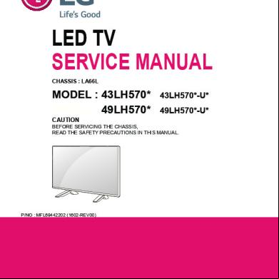
Lg+43lh570+chassis+la66l 526846
December 2019 53
Lg 50pc1dr Ua Service Manual 2x2u5f
February 2022 0More Documents from "Rosalino Leonides Martinez Marquez" 2e2z1c
Lg 26lh20 Ua Chassis La92a l722h
November 2019 47
St 4000 Plus 11r21
November 2019 48
Datos Generales Del Motor Sincronizacion De Ford 4.0 Lts 6r3ew
December 2019 49
Desperte Seu Poder.pdf 5o6k6s
July 2022 0
11482j
November 2019 33